In Electron Microscopy a beam of electrons (in place of light) and circular magnets (in place of glass lenses) permit the resolution of structures in much finer detail than in an optical microscope.
To have better understanding of electron microscope, Healthtard recommends to take the journey to optical light microscopy.
Wavelength of Electron microscope:
Visible light ranges in wavelength from the long red waves ( = 760 nm) to the short blue/violet waves ( = 400 nm). Ultraviolet waves can be as short as 230 nm. The wavelength of an electron beam depends upon its acceleration voltage, with the wavelength being given by Planck’s law.
For an electron of charge e, accelerated by a potential difference of V, is given by the formula:
For an electron microscope with 40,000 volts accelerating voltage, the wavelength of the electron would be 0.006 nm ((1.5/40,000) ).
).
Note that UV light increases the resolution by a factor of 2 over visible light, while the electron microscope has the potential to increase it by a factor of 10 to 10
to 10 over visible light.
There are two electron microscopes:
The first is a “traditional” transmission electron microscope (TEM) in which an electron beam passes through the specimen. The second is the scanning electron microscope (SEM) in which a beam of electrons scans the surface of an opaque object and produces an image of that surface.
Electron beam can not be seen directly by the human eye (it will injure the retina of the eye) nor can we see UV light. Thus, these forms of microscopy rely on photography, or upon fluorescent screens.
The images are viewed on a cathode tube, or in pictures taken with the microscope.
In the electron microscope, the ocular lens is replaced with a projection lens, since it projects an image onto a fluorescent screen or a photographic plate.
Since the electrons do not pass through glass, they are focused by electromagnetic fields. Instead of rotating a nose-piece with different fixed lenses, the EM merely changes the current and voltage applied to the electromagnetic lenses.
The size of an electron microscope is dependent upon two factors. Primary is the need for a good vacuum through which the electrons must pass (it takes less than 1 cm of air to completely stop an electron beam). Peripheral pumps and elaborate valves controls are needed to create the vacuum.
A substantial electrical potential (voltage) is also needed to accelerate the electrons out of the source. The source is usually a tungsten filament, very much like a light bulb, but with 40-150 Kilovolts of accelerating voltage applied to an anode to accelerate the electrons down the microscope column.
Modern electronics have produced transformers which are reasonably small but capable of generating 60,000 volts. Transformers used to be room sized (and a large room at that). The million-volt electron microscopes have transformers as large as buildings – in fact, the building housing such a microscope is for the most part a cover for the transformer. While electron microscopes work with high voltage, they use only milliamps of current through the electron gun.
With the need for mechanical stability that is imposed by resolution in the Angstrom range, electron microscopes are usually formidable instruments. Ideally they lie on their own shock mountings to isolate the instrument from building and ground vibrations.
The size and cost of an electron microscope is due primarily to the need for stability and maintenance of the vacuum. With advances in vacuum technology (similar to the microchip revolution in electronics), and perhaps with the ability to manufacture devices in deep space, the size (and cost) of electron microscopes should decrease.
Another characteristic of electron microscopes is that they are usually designed upside-down, similar to an inverted light microscope. The electron source is on top, and the electrons travel down the tube, opposite to light rays traveling up a microscope tube.
This is merely a design feature that allows the operator and technicians ease of access to its various components. The newer electron microscope is beginning to look like a desk with a TV monitor on it.
Until recently, the major advantage of an electron microscope also has been its major disadvantage. In theory, the transmission electron microscope should be capable of giving a resolution of several angstroms. This would give excellent molecular resolution of cell organelles.
However, as the resolution increases, the field of view decreases and it becomes increasingly difficult to view the molecular detail within the cell.
Electron microscopes designed to yield high resolution have to be compromised to view larger objects. Cell structures fall within the size range that was most problematic for viewing.
For example, if we wished to resolve the architecture of an entire eukaryotic chromosome, not just the chromosome, but the cell itself was too large to be seen effectively in an electron microscope. Zooming in on paired chromosomes was impossible.
Modern electron microscope design allows for this zooming, and the observation of whole tissues while retaining macromolecular resolution.
Resolution of an imaging system :
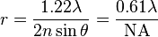
where,
 is the minimum distance between resolvable points, in the same units as
  is specified
- is the wavelength of light, emission wavelength, in the case of fluorescence,
 is the index of refraction of the media surrounding the radiating points,
 is the half angle of the pencil of light that enters the objective, and
 is the numerical aperture.
- NOTE: The details of the terms in the above formula are explained in this post.
Scanning Electron Microscopy (SEM)
The scanning electron microscope (SEM) uses a focused beam of high-energy electrons to generate a variety of signals at the surface of solid specimens.
The signals that derive from electron-sample interactions produces various signals that reveal information about the sample including external morphology (texture), chemical composition, and crystalline structure and orientation of materials making up the sample.
The most common SEM mode is detection of secondary electrons emitted by atoms excited by the electron beam. Number of secondary electrons depends on angle at which beam meets surface of specimen, i.e. on specimen topography.
By scanning the sample and collecting the secondary electrons with special detector, an image displaying the topography of the surface is created.
Scanning electron microscope
Transmission electron microscope:
The transmission electron microscope (TEM) is the workhorse of histology primarily because of its resolving power (3-10 Å), and its similarity to traditional light microscopy and histotechnique.
Negative stained TEM image of influenza virus
TEMs find application in cancer research, virology, material science as well as pollution, nanotechnology and semiconductor research.
Alternate modes of use allow for the TEM to observe modulations in chemical identity, crystal orientation, electronic structure and sample induced electron phase shift as well as the regular absorption based imaging.
TEM image of 20 nm Gold nanoparticles in solution
In TEM a beam of electrons is transmitted through an ultra-thin specimen, interacting with the specimen as it passes through.
An image is formed from the interaction of the electrons transmitted through the specimen; the image is magnified and focused onto an imaging device, such as a fluorescent screen, on a layer of photographic film, or to be detected by a sensor such as a CCD camera.
TEM Sample preparation:
Sample preparation for TEM broadly involves more time and experience than for most other characterization techniques. A TEM specimen must be approximately 1000 Å or less in thickness in the area of interest. The entire specimen must fit into a 3 mm diameter cup and be less than about 100 microns in thickness.
A thin, disc shaped sample with a hole in the middle, the edges of the hole being thin enough for TEM viewing, is typical.
The initial disk is usually formed by cutting and grinding from bulk or thin film/substrate material, and the final thinning done by ion milling.
Other specimen preparation possibilities include:
- Direct deposition onto a TEM-thin substrate (Si3N4, carbon); direct dispersion of powders on such a substrate.
- Grinding and polishing using special devices (t-tool, tripod)
- Chemical etching and electropolishing; lithographic patterning of walls and pillars for cross-section viewing
- Focused ion beam (FIB) sectioning for site specific samples.
Artifacts are common in TEM samples, due both to the thinning process and to changing the form of the original material.
For example surface oxide films may be introduced during ion milling and the strain state of a thin film may change if the substrate is removed.
Most artifacts can either be minimized by appropriate preparation techniques or be systematically identified and separated from real information.
The scanning electron microscope (SEM) is becoming increasingly popular with cell biologists because of its remarkable ability for quantifiable mapping of surface detail, along with improved resolution (30-100 Å ) and its ability to show 3D structure.
The transmission electron microscope is identical in concept to the modern binocular light microscope.
It is composed of a light source (in this case an electron source), a substage condenser to focus the electrons on the specimen, and an objective and ocular lens system.
References and Further Reading :
- http://web.stanford.edu/group/snl/tem.htm
- Gustavus Adolphus College Resources (http://homepages.gac.edu/~cellab/chpts/chpt1/intro1.html)
- NPTEL courses (http://nptel.ac.in/courses/103106075/39)


